nanotools usa
nanotools usa
  • Home
  • Products
    • Featured Probes
    • All Standard Probes
    • Build-A-Probe™
  • Company
    • About
    • Patented Technology
  • TrueDimensions™
  • Blog
  • Privacy
  • Home
  • Products
    • Featured Probes
    • All Standard Probes
    • Build-A-Probe™
  • Company
    • About
    • Patented Technology
  • TrueDimensions™
  • Blog
  • Privacy

Patented Technology
Electron beam induced processing

nanotools EBD Technology
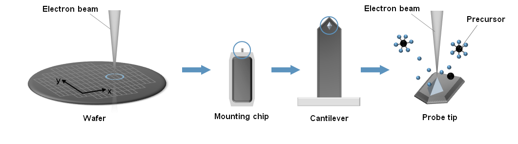
With more than 20 years of experience in developing and producing SPM tips by means of our patented electron beam induced processing (EBIP), we are able to control up to 50 fabrication parameters in order to achieve the highest dimensional and angular accuracies on the nanometer scale:
  • tip length accuracy better than ± 10% of the nominal tip length
  • tip shape accuracy better than ± 2 nm
  • tip apex sharpness down to < 2 nm
  • tip orientation accuracy better than ± 0.5°
Our EBIP approach opens up unique opportunities in terms of customizability and scalability at consistently high standards of quality and reliability — according to our quality management system certified according to ISO 9001.

Hours
M-F: 8am - 6pm PT

Phone
844-ebd-tips
844-323-8477

Email
info-usa@nanotools.com

Tip Handling
How to buy
Terms and conditions
Shipping Methods
Return/Refund
Privacy
Contact

Disclaimer
​Impressum​​
© 2022 nanotools USA LLC. All rights reserved.